Moore’s law, which states that the transistor density of integrated circuits will double every year, has slowed down. Many companies have attempted to combat this issue as the need for processing power increased. Despite a sharp increase in the costs of a new node, transistor density saw little improvement. While it was common for most companies to build a processing unit out of a monolithic die, other companies found improved yield and binning through breaking down large dies into smaller “chiplets”. According to AMD CEO Dr. Lisa Su, the cost per die doubles going from a 45 nm node to a 28 nm node and it quadruples going to a 7nm node. Moving to smaller nodes will only increase costs. For example, considering a medium-sized die of 18mm x 20mm (360mm2) on a standard wafer size of 300mm, up to 150 dies can be fabricated using this equation:

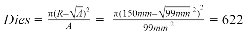
However, spitting up the same die into 4 chiplets results in 622 dies instead with a size of about 9.5mm x 10.5 mm (about 99mm2):
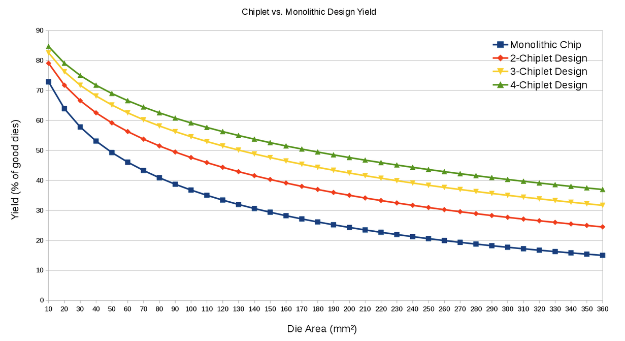
Although this might not seem like a large increase, the true value of chiplets lies in yield. With the die area of 360mm2, only 15% of dies are free of defects if it is based off a monolithic design. On the other hand, using the same die area, the yield can be increased to 37% using a 4-chiplet design given this graph.
Therefore, I believe a chiplet design is the most effective way in combating the slowing of Moore’s law.
